An introduction to electronic weighing

Weighing In
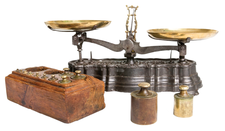
© Lead Image © Carlos Velayos, 123RF.com

© Lead Image © Carlos Velayos, 123RF.com

Author(s):

Create your own weighing device with easily available components and open source software.

In this article, I discuss the design of a compact and portable workshop balance for various single-load-cell weighing applications constructed with a small load cell, an instrumentation amplifier, an excitation supply, a microcontroller, a display, and a serial port for debugging. Throughout, I used Linux and open source software, and I provide code samples, with directions for finding the complete code online.

History

Ancient civilizations used simple balances to compare weights for trading in precious metals, spices, salt, and the like. Today's civilization is no less dependent on knowing the weight of objects. It is hard to imagine a day in which the knowledge of weight does not take part: from the morning visit to the bathroom scales, a trip to the supermarket, baking a cake, to weighing baggage at the airport – the list of times weight plays a part in our lives seems endless. Today, we've moved away from mechanical balances, for the most part, obviating the need for ready reference weights.

Today's weighing equipment is usually based on electronic signals from strain gauges. These sensors are thin-film resistors whose resistance varies in response to tension or compression. When bonded to a mechanical structure subject to the force of an applied mass, the resistance of a strain gauge will change proportionally in response. Practical weighing systems use more than one strain gauge, and these are generally bonded to a metallic billet in a controlled manner to form a more complex electrical circuit designed to eliminate nonlinearities and temperature effects. These billets are known as load cells and are available commercially with working ranges from a few grams to hundreds of tonnes.

Load cells (Figure 1) are built into the structures of complete weighing systems such as scales, weighbridges, hoists, and counting scales in such a way that they can be replaced easily should the need arise. Although load cells are transducers with no moving parts, of course they do deflect slightly under load, and that allows mechanical endstops to be used to limit the deflection and protect the cell from overload. It should be noted that larger weighing machines such as weighbridges will employ more than one load cell, a typical arrangement being a rectangular platform with a load cell at each corner. The signals from each load cell are summed electronically to provide a total weight. Often, a range of load cells of different capacities will share the same basic billet, machined in different ways.

Figure 1: A typical modern load cell. The strain gauges are covered with a white flexible coating to protect them.

Load Cell Operation

In most load cells, four strain gauges are employed – two in tension and two in compression – in a symmetrical manner to eliminate temperature effects (Figure 2). The strain gauges are arranged into a Wheatstone bridge (Figure 3).

Figure 2: The arrangement of the strain gauges on the load cell billet and the forces that act on them. The "dumbbell" shape cut out of the billet makes the metal thinner in the vicinity of the strain gauges, increasing sensitivity.
Figure 3: This electrical arrangement is attributed to Charles Wheatstone [1], a Victorian physicist. It is very useful in this type of measurement because it allows the user to "null out" the standing voltages in a system and thus make accurate measurements of small changes.

A strain gauge is a sensor whose resistance varies with applied force, so that if you can measure resistance, you can measure that force. The conducting material (often constantan) is deposited onto an insulating substrate such as polyimide. The conductor is designed in a serpentine shape (Figure 4) such that extension by applied force in the longitudinal direction is much higher than that in the lateral direction. This arrangement reduces sensitivity to off-axis load. Pads are provided at the ends of the conductor so that lead-out wires may be soldered or otherwise bonded to them.

Figure 4: Strain gauge conducting material design.

The Wheatstone bridge requires a voltage across it to provide an output, and that voltage is called the excitation voltage. The output of the bridge is a differential, which slightly complicates the electronics, as you will see later. At zero load, the difference between the two outputs should be zero, and as load is applied, one arm will go positive while the other goes negative. The differential output at full scale is measured in millivolts per volt (mV/V) (i.e., a ratio of output versus the excitation voltage). Excitation voltages are generally in the range of 5V to 20V, and a typical load cell might have an output of 2mV/V, making 20mV output at full scale for 10V excitation. From this, it can be seen that you are dealing with very small voltages, especially when you require high precision. The upside of this arrangement is that much the same electronics can be applied to a wide variety of different weighing applications, because the load cell's maximum output will be similar in all cases.

The nominal resistance of the strain gauges is on the order of a few hundred ohms, so a bridge made up of four 400-ohm gauges will have a resistance (R) of 400 ohms, as seen by the excitation supply; thus, it can be see that some power is required to excite the load cell, which can be a challenge for battery-operated systems. In this case, lowering the excitation voltage saves power at the expense of full-scale output and, ultimately, precision. Although increasing the excitation voltage might seem attractive from the point of view of increasing load cell output, there comes a point when the strain gauges will self-heat, causing local expansion of the load cell billet and the attendant inaccuracy.

In a little more detail, the output of the load cell can be calculated in the following manner: V-=R2/(R1+R2) x Vex, whereas V+=R3/(R3+R4) x Vex, so the differential output voltage is:

Tare and Span: Calibration

One factor that must be considered when choosing a load cell for an application is tare, which refers to the weight of any structure supported by the load cell before any object to be weighed is placed on it. This tare might be the mixing bowl on a kitchen scale before ingredients are added or the platform required to support a multitonne truck on a weighbridge. Tare can represent a large portion of the ultimate full-scale range of a system and must be taken into account at the design stage.

Further removal of tare is sometimes required during normal operation: Again, using the example of a weighbridge on which a truck is to be loaded with goods, the initial zero point would be with the weighbridge empty. Once an empty truck is driven onto the weighbridge, it is convenient to again "zero" the weight display so that as goods are added to the truck, the display reflects what has been added, without the complication of the truck's tare. In the case of a weighing system designed to dispense ingredients in a fixed ratio (batch weighing) into a vessel (e.g., flour, water, yeast, and sugar in a bakery), the tare may be reset several times as the batch is assembled with the different ingredients.

"Span" is the term used to describe the full range of a weighing machine. The desired span is application dependent, and the load cell(s) must be chosen to have sufficient capacity for the required span plus tare, as described above. The stated output of the load cell at full scale is generally a nominal figure only, meaning the instrument must be calibrated before use at intervals during its operational life because of various mechanical and temperature effects. For a small instrument, this is a simple undertaking, reference weights being readily available at varying levels of precision from commercial sources [2], some of which can be traced back to national and international standards bodies.

For larger systems, calibration can be a complex and expensive exercise because you have no way to avoid the use of dead weights for calibration, and moving such weights around is time consuming and expensive.

Precision

Precision of a weigh scale is often quoted in "counts." For example, in a machine designed to weigh up to 10kg at 10,000 count precision, the least significant digit would represent 1g. In reality, precision at this level is difficult to achieve and often not required. If the load cell in such a machine has an output of 10mV at full scale, one count is represented by 1µV. Such low-level signal changes can be difficult to detect, especially in the presence of electrical noise and, indeed, vibration from the surrounding environment, which can render the weight signal unstable to begin with. Long-term stability of the load cell itself (known as creep), temperature effects, and tiny voltages generated between dissimilar metals in the wiring between the load cell and the amplifier can all contribute to errors in measurement and mandate regular calibration of the machine, especially if it is used at a point of sale. In these cases, various regulatory bodies [3] enforce calibration intervals to ensure customers get what they pay for.

Workshop Weighing System

As an example design, I wanted to produce something compact and portable that might prove useful in my workshop. I found a small load cell, freely available on eBay.com or other online sources, with a capacity of 100g (3.5oz) at low cost. The load cell is physically quite small (5x1x0.6cm) and easy to mount, and at such low capacity, it is easy to assemble into a plastic enclosure to produce a practical instrument. The load cell is one of a family of force transducers, so it would be easy to adapt the design to weigh heavier items for different applications.

The electronic design comprises four basic elements: an instrumentation amplifier, an excitation supply, a microcontroller, and a display.

Analog Front End

A number of application-specific integrated circuits are available for weigh scale applications that comprise a differential instrumentation amplifier and a 24-bit sigma-delta analog-to-digital converter (ADC). Some of these integrate other functions, such as an excitation regulator, but in essence, they perform the same task.

One of the most popular of these ADCs for weigh scales is the HX711 [4] from Avia Semiconductor, a Chinese company. It is readily available from Alliexpress.com and eBay.com, both as a bare chip and mounted on a simple printed circuit board (PCB). I assume this chip forms the basis of many of the kitchen scales and the like manufactured in China. I did some initial prototyping with this chip, and it seems very capable. Certainly, if you want to hook up a load cell to an Arduino or a Raspberry Pi, the datasheet provides example drivers in C and assembler, and you can get something up and running in a few minutes.

An alternative part from a more established manufacturer is the ADS1232 [5] from Texas Instruments. This part is available through more traditional distribution, such as mouser.com and digikey.com. The datasheet (and associated application notes) is somewhat more detailed, with an application circuit provided for a weigh scale. The ADS1232 lacks the excitation regulator of the HX711, but that in itself has some limitations, and a separate excitation regulator is not difficult to implement and is more flexible and potentially more stable. Interestingly, both of these chips have a very similar digital interface, suggesting they share a common heritage.

My choice for this design was the somewhat more expensive ADS1232 with a separate excitation regulator implemented with a REF5040 [6] (also from Texas Instruments), a high-stability reference supply chip capable of supplying 4V at 10mA directly to the load cell.

Display

For the display, I wanted a large, bright, clear output that was cost effective. I also wanted something that was easy to drive and required few pins from the microcontroller. The display I chose was a six-digit LCD with a white LED backlight from Hobby Components [7] that requires only three lines to drive. The digits are about 1.5cm (0.6in) in height, with a battery state indicator to the right of the display. It is based on the HT1621 chip by Holtek [8], and the datasheet is available from their website.

Microcontroller

Once all the other parts of the design were chosen, attention could turn to selecting a suitable microcontroller. Because I'm already familiar with ST Microelectronics' range of ARM-based controllers, this was an obvious place to start. However, I also wanted a low-cost solution that was scaled appropriately for this application. I was pleasantly surprised to find that the ST's "Value Line" controllers include a device that runs at 48MHz without an external crystal, has 20 pins (plenty for this application), and 16KB of flash program memory. Programming and debugging use ST's two-wire ST-Link interface, and a Linux-based IDE, the STM32CubeIDE, integrates well with ST-Link. This device is available for less than a dollar. USB-based ST-Link programmers are available online for just a few dollars, as well. The exact device is the STM32F030x4 [9].

Design

Schematic capture and PCB layout were both performed by KiCad, a free and open source CAD tool originally developed at CERN [10]. It really is an excellent suite of tools and handles the entire process of electronic design from schematic capture (Figure 5) right through to generating files for manufacture. It even has a 3D viewer that generates a panable/rotatable image of your design, including the components. Although PCB assemblies are in some ways two dimensional, the use of the 3D viewer has saved me from mechanical clashes that are not apparent from the two-dimensional design perspective. You can export the 3D model as a STEP file and import that into 3D CAD tools such as FreeCAD to build up more complex assemblies (e.g., aiding the design of parts suitable for 3D printing, such as enclosures).

Figure 5: The full schematic for the final design.

Many excellent PCB companies online will build good-quality PCBs in a few days for less than $5 (EUR6, £5), so building prototypes or experimental PCBs is not prohibitively expensive.

A four-pin terminal block is provided for connecting the load cell: two excitation pins and two signal pins. The excitation is provided by the REF5040, and the signal pins go to the ADS1232 through a simple low-pass filter. The ADS1232 needs a handful of passive components for filtering and stability, and its digital interface is three lines that go directly to the microcontroller. The microcontroller in turn drives the display with its three-line interface, with enough spare I/O pins on the controller to provide additional facilities (i.e., a battery monitoring circuit, a temperature input from the REF5040, a serial port for debugging and/or data logging, and two buttons used for tare and span setting). A pin switches or dims the display backlight.

Power is supplied by a PP3 (9V) battery, and two linear regulators provide 3.3V for the digital electronics and 5V for the analog section, giving some isolation between the two to minimize the effects of digital electrical noise. The 5V analog supply allows the REF5040 to generate a stable 4.1V for the load cell excitation. The 9V supply greatly simplifies the power supply design, allowing the use of linear regulators. If a lower supply were used (e.g., two lithium ion cells), some form of switching regulator would be required to boost the voltage to a level suitable for the load cell excitation, with all the attendant noise problems that could bring.

The PCB layout itself is fairly straightforward. Having decided the display would mount directly above the PCB, I saw that it was fairly apparent that most components could go under the display, with only switches and connectors requiring a margin around the edge. Therefore, I arrived at a size of 100x50mm (4x2 inches), with a two-layer PCB being more than adequate for such a simple circuit. Close attention was paid to layout of the analog section, care being taken to distance it from digital lines where possible, placing decoupling capacitors close to the analog chips and creating generous ground planes on the top and bottom layers. A 3D rendering of the resulting PCB is shown in Figure 6.

Figure 6: A 3D view of the load cell PCB.

Software Development

The use of IDEs can be controversial and very much a matter of taste, and it's certainly possible to do this type of microcontroller development without one. The ARM compilers and standard libraries can be downloaded from your distro's repository, and you're off, using any editor that suits you and Make or Cmake – again, your choice. Once you have a compiled binary, utilities for ST-Link allow you to program your device, and you can use GDB (the GNU debugger) to debug you program.

That said, ST's STM32CubeIDE, based on Eclipse, does streamline the process by integrating ST's CubeMX tool, a utility that allows you to configure your microcontroller and generate a software framework that does all the initialization and leaves you with a blank main() function to add to your code. You can label the pins of the microcontroller (bonus points if you use the same names as on the schematic!).

The pin configuration for this design is shown in Figure 7. Once saved, the IDE generates a set of #define directives for the I/O pins that you can use in your code and a complete set of initialization routines. At this point, you can continue to use the IDE or ignore it and use Make with the generated makefile. However, if you stay with the IDE and have your hardware connected by an ST-Link programmer, a single mouse click compiles, downloads, and runs your code. This level of preconfiguration – including, if you want, the inclusion of a real-time operating system (RTOS) such as FreeRTOS – can leave you free to concentrate on your application code. In a commercial environment, time to market is everything, and time savings like this can be invaluable.

Figure 7: The project pin configuration in STM32CubeIDE.

Serial I/O and printf

My hardware design and microcontroller configuration includes a serial port for debugging. Being able to output data and wait for keystrokes during debugging can be invaluable as an alternative to, or as an adjunct to, a debugger. The STM32 libraries make it easy to override the low-level routines that printf and scanf eventually call and redirect them to a serial port (Listing 1). Once this is done, these functions are available from whatever terminal (e.g., the Linux minicom tool) you choose to connect to the serial port. This serial port could also be used in an application for batch weighing, in which an external computer or programmable logic controller (PLC) monitors the weight signal on a continuous basis.

Listing 1

Overriding Low-Level I/O Primitives

01 /** read from the serial port */
02 int _read(int file, char *ptr, int len)
03 {
04   HAL_UART_Receive(&huart1, (uint8_t *)ptr, 1, -1);
05   return 1;
06 }
07
08 /** write to the serial port */
09 int _write(int file, char *ptr, int len)
10 {
11   int DataIdx;
12
13   for (DataIdx = 0; DataIdx < len; DataIdx++)
14   {
15       if (*ptr == '\n')
16       {
17           HAL_UART_Transmit(&huart1, (uint8_t *)"\r\n", 2, -1);
18       }
19       else
20       {
21           HAL_UART_Transmit(&huart1, (uint8_t *)ptr, 1, -1);
22       }
23     ptr++;
24   }
25   return len;
26 }
27
28 /** wait for a keystroke */
29 uint8_t kbhit(void)
30 {
31     return __HAL_UART_GET_FLAG(&huart1, UART_FLAG_RXNE);
32 }

ADC Driver

The ADS1232 has a very simple two-wire serial interface with no configuration registers, so all setup (clock speed, gain, etc.) happens from pins on the chip. To read the data from the chip, the software must first wait for a valid sample, which it does by waiting for the DOUT (data out) line to go low (Listing 2). At this point, data is clocked out in a serial manner by pulsing the clock pin from low to high and reading the resulting data bit from DOUT. This process is repeated 24 times to clock out a complete 24-bit sample. A further clock pulse resets DOUT to its "data ready" function.

Listing 2

Reading the ADC

01 /** wait for ADC sample ready and read it out */
02 uint32_t ADS1232_Read(void)
03 {
04   int32_t value = 0;
05
06   // wait for DOUT to go low : data ready
07   while (HAL_GPIO_ReadPin(ADC_NDRDY_DOUT_GPIO_Port, ADC_NDRDY_DOUT_Pin))
08     ;
09
10   for (uint8_t i = 0; i < 24; i++)
11   {
12     value = value << 1;
13
14     // send clock pulse
15     HAL_GPIO_WritePin(ADC_SCLK_GPIO_Port, ADC_SCLK_Pin, 1);
16     HAL_GPIO_WritePin(ADC_SCLK_GPIO_Port, ADC_SCLK_Pin, 0);
17
18     // read the data in
19     if (HAL_GPIO_ReadPin(ADC_NDRDY_DOUT_GPIO_Port, ADC_NDRDY_DOUT_Pin))
20     {
21       value |= 1;
22     }
23   }
24
25   // reset DOUT
26   HAL_GPIO_WritePin(ADC_SCLK_GPIO_Port, ADC_SCLK_Pin, 1);
27   HAL_GPIO_WritePin(ADC_SCLK_GPIO_Port, ADC_SCLK_Pin, 0);
28
29   // 24-32 bit 2s complement conversion
30   value <<= 8;
31   value /= 256;
32
33   return (value);
34 }

Filtering Data

Before displaying the data, some sort of filtering is usually required that removes fluctuations in the weight display caused by noise and vibration, but filtering comes at the cost of response time. The raw samples from the ADC take 100ms to acquire, so any form of low-pass filtering will slow down the response time into the region by fractions of a second. In the case of a workshop balance, a couple of seconds for the reading to settle is not a problem, but in other cases (e.g., a batch-weighing application), every second adds to production time and therefore costs money. Filtering and ultimate accuracy will always be a trade-off. In this application, 10 samples are simply averaged before the result is passed for display (Listing 3).

Listing 3

Averaging ADC Readings

01 #define SAMPLES 10
02
03 int32_t samples[SAMPLES];
04 int32_t average = 0;
05 uint8_t sample = 0;
06
07 // main acquisition loop
08 while (true)
09 {
10   samples[sample++] = ADS1232_Read();
11   if (sample == SAMPLES)
12   {
13     sample = 0;
14   }
15
16   average = 0;
17   for (uint8_t i = 0; i < SAMPLES; i++)
18   {
19     average += samples[i];
20   }
21
22   average /= SAMPLES;
23
24   // pass the averaged data to the display here
25 }

Practical Precision

In terms of practical precision, you must keep a few things in mind. Of the theoretical 24 bits of precision available from the ADC, the datasheet itself admits that only 19 bits are useful at the highest gain setting. The load cell I have chosen has a maximum output of 4mV (1mV/V, with an excitation of 4V), so it uses only one fifth of the available range (20mV) of the ADC. That's about 100,000 counts. Practically, I have found I can achieve stable readings to 10,000 counts. For a 100g scale, that means one count is equivalent to 10mg. The current software limits that further, giving a resolution of 100mg (i.e., 1,000 counts), which seems more than adequate for the requirements of a general-purpose laboratory scale. There is certainly scope for better filtering and other techniques to improve the precision, but at some point the limitations of the (cheap) load cell will become the limiting factor.

Display Driver

The display has a three-wire serial interface. The chip select (CS) line must be asserted before data can be written, and once that is done, data is presented on the data (DAT) line, being clocked into the chip by asserting the write (WR) line and then negating it (Listing  4). The interface is too slow to keep up with the microcontroller at full speed, so busy-wait loops are necessary to slow the WR line pulses down to just over 3µs.

Listing 4

Writing a Single Bit to the Display

01 /** */
02 static void LCD_WriteBit(bool bit)
03 {
04   // set the data line
05   HAL_GPIO_WritePin(LCD_DAT_GPIO_Port, LCD_DAT_Pin, bit);
06
07   // assert the WR line
08   HAL_GPIO_WritePin(LCD_NWR_GPIO_Port, LCD_NWR_Pin, 0);
09
10   // busy wait
11   for (uint8_t i = 0; i < 50; i++)
12     ;
13
14   // negate the WR line
15   HAL_GPIO_WritePin(LCD_NWR_GPIO_Port, LCD_NWR_Pin, 1);
16
17   // busy wait
18   for (uint8_t i = 0; i < 50; i++)
19     ;
20 }

The display chip has a small amount of internal memory, and the individual bits in this memory correspond to the different segments in the display characters, as well as decimal points and the battery state indicator. Each transaction with the chip is called a command, and the first three bits of that command determine the type of command. The rest of the transaction comprises an address in the internal memory and the data to be written.

The process of writing a complete digit involves conversion from the required ASCII digit to the memory bit pattern to illuminate the display correctly. This code is not complex, but quite long, so I won't include it here. I refer the interested reader to the source code on my GitHub page [11].

Storing Calibration Parameters

The design provides no non-volatile storage for persistent data such as calibration parameters. In a larger system, it is customary to have an external SPI flash memory or EEPROM chip to provide this function. The current design uses a small portion (one page, 1KB) of the microcontroller's program flash memory as non-volatile storage (Listing 5), and you can tell the linker to exclude a portion of this flash memory from program memory (usually a page at the highest address available). That block can then be labeled in the linker file so that it is accessible from program code, and primitives in the STM32 libraries can erase pages and read/write bytes or words from that area. This technique saves the expense of an external memory chip and the I/O pins that would be required to drive it. Listing 6 from the linker file shows how to reserve a portion of flash memory for parameter storage.

Listing 5

Nonvolatile Storage Code

01 /*
02  * nvdata.c
03  *
04  *  Created on: 19 Mar 2021
05  *      Author: andrew
06  */
07
08 #include "main.h"
09
10 extern uint32_t _nvdata[1024]; // start of non-volatile data (last block of main flash) defined in linker file
11
12 /** */
13 void NVDATA_SaveCalibrationParams(uint32_t span, uint32_t zero)
14 {
15   HAL_FLASH_Unlock();
16
17   FLASH_EraseInitTypeDef eraseInit;
18
19   eraseInit.TypeErase = FLASH_TYPEERASE_PAGES;
20   eraseInit.NbPages = 1;
21   eraseInit.PageAddress = (uint32_t)&_nvdata[0];
22
23   uint32_t sectorError;
24   printf("erasing flash page at %p\n", &_nvdata[0]);
25   HAL_StatusTypeDef res = HAL_FLASHEx_Erase(&eraseInit, &sectorError);
26
27   if (res != HAL_OK)
28   {
29     printf("FLASH erase error %d\n", res);
30   }
31
32   res = HAL_FLASH_Program(FLASH_TYPEPROGRAM_WORD, (uint32_t)&_nvdata[0], span);
33
34   if (res != HAL_OK)
35   {
36     printf("FLASH program error %d\n", res);
37   }
38
39   res = HAL_FLASH_Program(FLASH_TYPEPROGRAM_WORD, (uint32_t)&_nvdata[1], zero);
40
41   if (res != HAL_OK)
42   {
43     printf("FLASH program error %d\n", res);
44   }
45
46   HAL_FLASH_Lock();
47 }
48
49 /** */
50 void NVDATA_LoadCalibrationParams(uint32_t *span, uint32_t *zero)
51 {
52   *span = _nvdata[0];
53   *zero = _nvdata[1];
54 }

Listing 6

Linker File Extract

01 /* Entry Point */
02 ENTRY(Reset_Handler)
03
04 /* Highest address of the user mode stack */
05 _estack = ORIGIN(RAM) + LENGTH(RAM);  /* end of "RAM" Ram type memory */
06 _nvdata = ORIGIN(NVDATA);
07
08 _Min_Heap_Size = 0x200 ;  /* required amount of heap  */
09 _Min_Stack_Size = 0x400 ; /* required amount of stack */
10
11 /* Memories definition */
12 MEMORY
13 {
14   RAM    (xrw)    : ORIGIN = 0x20000000,  LENGTH = 4K
15   FLASH  (rx)     : ORIGIN = 0x8000000,   LENGTH = 15K //reduce flash by 1K
16   NVDATA (rx)     : ORIGIN = 0x8003c00,   LENGTH = 1K //define the nv region
17 }
18
19 /* Sections */
20 SECTIONS
21 {
22  ### ommited ###
23
24   .nvdata : // give the nv region a name so it can be referenced from code
25   {
26     KEEP(*(.nvdata))
27   } >NVDATA
28
29  ### ommited ###
30 }

Calibration

The design has two push buttons for calibration: one for tare and one for span. In the main acquisition loop (Listing 7), the code looks for push-button events. If the tare button is pushed, the current reading is stored and subtracted from subsequent readings to provide a zero output. Similarly, if the span button is pushed, the required span factor is calculated and stored (in this case, the code assumes a 100g calibration weight has been placed on the scale).

Listing 7

Calibration

01 int32_t zero = 0;
02 int32_t span = 1;
03
04 // main acquisition loop
05 while (true)
06 {
07   // get averaged data here
08
09   if (sw1PushedEvent())
10   {
11     zero = average;
12     NVDATA_SaveCalibrationParams(span, zero);
13   }
14
15   if (sw2PushedEvent())
16   {
17     raw = (average - zero) * 100;
18
19     span = raw / 1000;
20
21     NVDATA_SaveCalibrationParams(span, zero);
22   }
23
24   display = ((average * 100 - zero * 100) / span);
25
26   LCD_PrintNumber(display, 0);
27 }

Completed Unit

I used FreeCAD to design an enclosure for the completed instrument and had it printed by a local 3D printing house. FreeCAD is another open source package, and every time I return to FreeCAD, I find the developers have made another step increase in functionality. It really is an exemplary open source project. The STEP files created were sent directly to a local 3D print house and were printed in just a few days.

I purchased a suitable stainless steel pan with a tare weight of just 50g, and the completed assembly can be see in Figure 8. I've left off the front panel to show the mounting arrangement of the PCB and the display. The load cell is mounted behind, with a vertical riser coming up through an aperture in the enclosure. A small circular plastic plate is attached to that, on which the pan sits.

Figure 8: The 3D-printed enclosure with the front panel removed.

Wrap-Up

I've presented here some background on the theory and application of industrial weighing. I've shown a practical design for a workshop balance that is flexible enough to be applied to many single-load-cell weighing applications and, in the process, shown that Linux and open source software make an excellent choice for engineering applications. I hope this example encourages you to experiment with strain gauges and load cells and come up with your own innovative applications. The complete design is available on my GitHub page, and I can be contacted by email (see my bio).

Finally, I'd like to dedicate this article to my father, who started and ran his own industrial weighing company for many years and taught me much of what I know.

The Author

Andrew Malcolm (MIET, CEng) works as a lead hardware and firmware engineer for Guru Systems (https://www.gurusystems.com/), a fast-growing IoT hardware and SaaS company working on low-carbon-energy projects. In his spare time, he likes to combine software engineering with his first love, hardware engineering. With all the open source tools available, he is never short of things to design. The Raspberry Pi has proved to be a source of inspiration, and to date, Andrew has designed five different add-ons, or HATs. He is currently working on microstepping motor drives for a Pi-based laser cutting machine. You can contact him at mailto:andrewrussellmalcolm@gmail.com.