
Designing field-programmable gate arrays
Planting Trees

© Lead Image © Anastasiya Zabolotnaya, 123RF.com
Learn what FPGAs are, how they work, and how to design FPGA integrated circuits on Linux.
In 2023, the number of people who have written some form of software code at least once is surely orders of magnitude greater than whatever it was in 1991, when Linux was born. That is good, but in my opinion, another very important group should have grown even more in the same period, but didn't: I refer to the people who have tried at least once to design digital integrated circuits (ICs) – that is, digital hardware instead of software.
This is a pity, because without such circuits no software could exist, and designing them is much more accessible today than it was 30 years ago. My goal in this article, which requires no previous knowledge of digital ICs, is to prove that point – at least for those really important ICs (that can also run Linux), known as field-programmable gate arrays (FPGAs).
The basic flow and core concepts of FPGA design are not intrinsically more difficult than those for efficient software design. However, they are different enough that a complete FPGA tutorial for beginners could well fill half this magazine.
Instead, to tempt even people who have never heard of FPGAs to try designing them, I deliberately cover just the bare minimum necessary to do two things:
- Understand what ICs really are, why FPGAs exist, how they work, and why they must be designed in a certain way.
- How to try the design flow on any Linux computer, before actually buying an FPGA development board. In this part, I show how to install the free editions of the two most important FPGA design environments these days and give a high-level overview of FPGA design flows and FPGA design languages. In a follow-up article, I will describe how to simulate an FPGA design to test its correctness.
Digital IC Building Blocks
Digital electronic chips are combinations of a few basic building blocks. The common characteristic of those blocks, called logic gates, is that all their input and output signals can only be in one of two states, normally high or low voltage, conventionally represented as TRUE or FALSE or as 1s or 0s.
To clarify this concept, consider the several views of the logic gate called NOT-AND (NAND), a basic circuit that "produces an output which is false (0) only if all its inputs are true" [1], according to its truth table in Table 1. Figure 1 shows the several levels of abstraction of a NAND logic gate, down to its physical implementation on silicon.
Table 1
NAND Truth Table
| Input |
| Output |
|---|---|---|
| A |
B |
A NAND B |
| 0 |
0 |
1 |
| 0 |
1 |
1 |
| 1 |
0 |
1 |
| 1 |
1 |
0 |
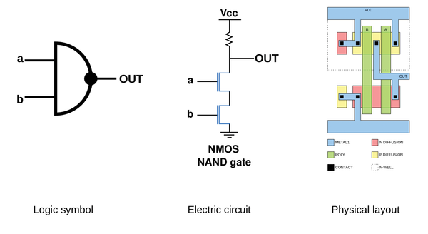 Figure 1: The NAND gate is the basic building block of digital microelectronics.
The drawing on the left in Figure 1 is the symbol that represents one NAND gate in functional diagrams. The electric circuit in the middle shows how to connect two of the microswitches, known as transistors, both to each other and to power or ground lines, to implement the NAND behavior of Table 1: Only when both transistors are "open" (by turning "on," i.e., applying high voltage to control pins a and b) is the OUT pin connected directly to ground – that is, low voltage or FALSE (0).
The rightmost part of Figure 1 shows one way to connect microscopic stripes of metal and semiconductors on a silicon wafer to create the physical equivalent of the electric NAND circuit to its left.
The NAND gate is important because "any boolean function can be implemented by using a combination of NAND gates" [1].
Repeat this millions of times: Connect all the gates to each other with microscopic stripes of metal and clock signals that synchronize all transitions from one state to another, and you get modern ICs. These tiny squares encased in flat plastic can perform, in an extremely reliable way, any function that can be expressed in boolean format – that is, processing sequences of 1s and 0s. Those silicon matrices of many millions of logic gates form the core of all digital ICs, from Arduino microcontrollers to all the CPUs in all computers and smartphones and from GPUs to the custom chips that mine bitcoins.
Benefits of Digital ICs
The advantage of digital hardware over any software that can do the same job running on any general-purpose CPU is inherently parallel processing, which takes place at constant, much higher speeds, with much smaller power consumption. Almost always, with software, you only get the appearance of multitasking, as the CPU continuously switches from running instructions of one program to running instructions of another program, or kernel code – so fast than you might never notice the alternation – until even the CPU can't keep the pace anymore.
Instead, inside gate arrays, all the modules that correspond to some logical function work in a totally parallel fashion, exactly because they are independent physical circuits and not bundles of instructions competing for processor time.
In the same gate array, you might have a few square millimeters of logic gates that compress images all the time while the surrounding modules each do something completely different (e.g., anything from transmitting data over Ethernet to calculating square roots) regardless of the load on all the other blocks. As I already mentioned, synchronous operations and constant performance are guaranteed because logic gates can be set to change state only at fixed intervals on the transitions (edges) of a common clock signal.
The price to pay for all this performance is immutability: Until they physically break, RAM modules can only be RAM modules that just store bits, CPUs can only recognize and execute one predetermined set of machine code. Modem controllers cannot become GPUs for gamers and vice versa. In general, those and all other so-called application-specific integrated circuits (ASICs) can only do the one job they were designed to do and nothing else, ever, because all the connections among single logic gates that transform a generic gate array into a specific IC are permanent and created during manufacturing.
An obvious, very troublesome consequence of this immutability is that you cannot "patch" errors in the placement or connections of some logic gate inside a gate array as you could patch, recompile, and reload software shipped with some bug. When a hardware error happens, you must throw that chip away and make a new one. Because of the complexity of today's ASICs, this means the tiniest error in the design and manufacturing of a prototype can cost millions of dollars and weeks of delay.
Then Came FPGAs …
FPGAs (Figure 2) were invented just to avoid the risks and limitations discussed. They are ICs that give up a non-negligible amount of gate density, maximum speed, and power consumption optimizations in exchange for huge flexibility, at a level that software alone may never reach.
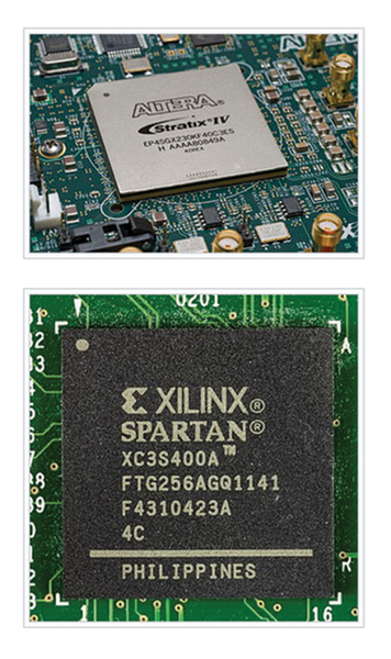 Figure 2: FPGA chips, like the Stratix IV from Altera (top) and the Spartan from Xilinx (bottom), can become any digital circuit you want (and run Linux, too). Altera image CC BY 3.0 [2]; Xilinx image CC BY-SA 4.0 [3].
Inside an FPGA, each cell of its gate array is surrounded by, and attached to, extra wires, microswitches, and other circuitry that can connect it to any of the other cells in a non-permanent way. The connections are enabled or disabled according to the instructions that the FPGA automatically downloads as a "programming file" every time it is powered up from an external memory chip that you can rewrite at will.
Therefore, if you need to fix a bug in an FPGA you already soldered to a board or you need to implement new, completely different functions inside it, you just load different instructions in that memory and power cycle the board: When it comes up again, the FPGA chip will be a completely different piece of digital hardware.
The only things you cannot change are the maximum clock speed, the number and nature of pins, and the pin connections to the rest of the host board. Internally, however, the FPGA can be any circuit you want, as long as it's feasible with the amount of transistors it contains and you respect all the design constraints. Modern FPGAs are so big and powerful that you might even include in their designs whole processors able to run Linux. (See the "Linux Inside FPGAs" box.)
Linux Inside FPGAs
Many people know that the Linux kernel can be tuned to run in very small processors for all sorts of embedded applications. What is less known is that, when designing a modern FPGA, you can, just as a software programmer does with software libraries, "load" turnkey designs of small CPUs called "soft processors," so-called because you "load" them inside a bigger circuit, instead of buying and mounting them as separate chips.
Both Altera and Xilinx have their own soft processors called Nios [4] and MicroBlaze [5], respectively, that can run custom versions of Linux, among other things. Their use inside FPGAs is facilitated by development platforms like PetaLinux [6], which is built on top of the Yocto Linux distribution. PetaLinux tools allow quick generation of custom Linux systems or just kernel images for Xilinx boards, complete with device drivers and testing tools, both for simulation and for the real hardware.
The flexibility of FPGAs enables rapid, inexpensive prototyping of any complex custom logic and makes it possible to sell and deploy hardware products whose hardware functions can be upgraded remotely, without any manual intervention on the chips themselves or the boards that host them. Even more important, for the purposes of this article, this same flexibility makes FPGAs excellent learning tools for digital IC design.
If you need one more reason to realize the importance of FPGAs and why it might be a good career move to know them, consider this: In the last decade, the two biggest manufacturers of FPGAs, Altera and Xilinx, were acquired by none other than Intel and AMD, respectively.
Buy this article as PDF
(incl. VAT)
Buy Linux Magazine
US / Canada
UK / Australia
Subscribe to our Linux Newsletters
Find Linux and Open Source Jobs
Subscribe to our ADMIN Newsletters
Support Our Work
Linux Magazine content is made possible with support from readers like you. Please consider contributing when you’ve found an article to be beneficial.

News
-
So Long Neofetch and Thanks for the Info
Today is a day that every Linux user who enjoys bragging about their system(s) will mourn, as Neofetch has come to an end.
-
Ubuntu 24.04 Comes with a “Flaw"
If you're thinking you might want to upgrade from your current Ubuntu release to the latest, there's something you might want to consider before doing so.
-
Canonical Releases Ubuntu 24.04
After a brief pause because of the XZ vulnerability, Ubuntu 24.04 is now available for install.
-
Linux Servers Targeted by Akira Ransomware
A group of bad actors who have already extorted $42 million have their sights set on the Linux platform.
-
TUXEDO Computers Unveils Linux Laptop Featuring AMD Ryzen CPU
This latest release is the first laptop to include the new CPU from Ryzen and Linux preinstalled.
-
XZ Gets the All-Clear
The back door xz vulnerability has been officially reverted for Fedora 40 and versions 38 and 39 were never affected.
-
Canonical Collaborates with Qualcomm on New Venture
This new joint effort is geared toward bringing Ubuntu and Ubuntu Core to Qualcomm-powered devices.
-
Kodi 21.0 Open-Source Entertainment Hub Released
After a year of development, the award-winning Kodi cross-platform, media center software is now available with many new additions and improvements.
-
Linux Usage Increases in Two Key Areas
If market share is your thing, you'll be happy to know that Linux is on the rise in two areas that, if they keep climbing, could have serious meaning for Linux's future.
-
Vulnerability Discovered in xz Libraries
An urgent alert for Fedora 40 has been posted and users should pay attention.